Top 10 Tips to Optimize PCB Design for Power Applications
The PCB design for power applications is a multifaceted process that requires careful attention to electrical, thermal, and mechanical considerations.
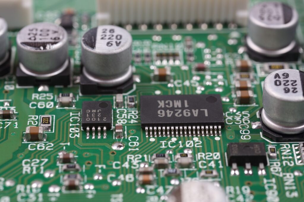
Top 10 Tips to Optimize PCB Design for Power Applications
1 – Understand the requirements
Before beginning a PCB design for power applications, it is crucial to understand the specifications fully. This involves considering voltage levels, current requirements, thermal considerations, and electromagnetic compatibility (EMC) constraints. Engineers should define key parameters such as input and output voltages, power levels, and environmental operating conditions. Understanding these parameters ensures the design will meet performance and safety requirements.
2- Layer Stack-up and grounding
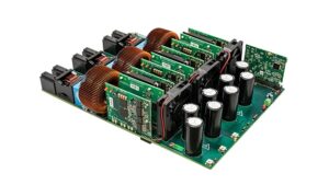
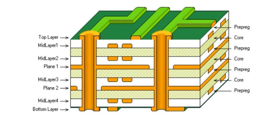
Multilayer boards (Figure 1) are highly recommended for power designs, as they allow for better noise management, reduced impedance, and optimized thermal performance. A dedicated ground plane, ideally on an uninterrupted layer, is essential for minimizing ground noise and providing efficient return paths. Separate planes for power distribution improve current handling and reduce voltage drops. A proper layer stack-up helps ensure that the design can handle the high currents and thermal challenges typically associated with power applications.
3 – Component placement
The placement of components on the PCB is critical to achieving reliable and efficient operation. Power-critical components such as MOSFETs, inductors, and power ICs should be placed close to each other to minimize trace lengths and associated losses. Components generating significant heat, such as power MOSFETs or linear regulators, should be positioned to facilitate effective heat dissipation through thermal vias or heatsinks. Additionally, sensitive analog or low-power digital sections should be placed away from high-power and high-frequency components to avoid interference.
4 – Routing guidelines
Trace routing plays a significant role in ensuring power integrity. Traces carrying high current should be wide enough to minimize resistance and voltage drop, with their dimensions calculated using standards like IPC-2221. Short and direct paths are essential for high-current routes to reduce inductive and resistive losses. Precision measurement in feedback loops can be achieved using Kelvin sensing techniques. To minimize electromagnetic interference (EMI), engineers should reduce the loop area of high-current paths and ensure proper grounding practices.
5 – Thermal design considerations
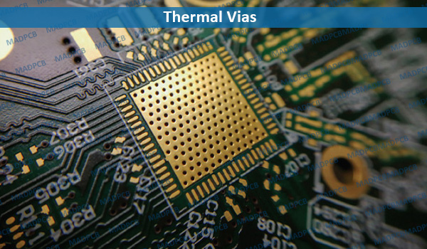
Managing heat is a critical aspect of power PCB design. Thermal vias can be employed to conduct heat away from hot components to internal layers or external heatsinks. Increasing the copper area around high-power components helps spread heat more effectively. Thermal simulations should be performed during the design process to identify and mitigate potential hotspots. Ensuring effective thermal management enhances the reliability and longevity of the PCB.
6 – Decoupling and filtering
Decoupling capacitors are indispensable for stabilizing voltage and reducing noise. These capacitors should be placed as close as possible to the power pins of ICs to ensure optimal performance. EMI filters, such as LC or pi-filters, can be added to input and output lines to suppress noise. Ferrite beads can also be used to reduce high-frequency noise on power lines, contributing to cleaner operation and better EMC performance.
7 – Design for manufacturability (DFM)
Designing with manufacturability in mind ensures that the PCB can be produced efficiently and cost-effectively. Components should be spaced adequately to accommodate automated pick-and-place machines. Thermal relief patterns for through-hole pads can simplify the soldering process. Conducting a Design Rules Check (DRC) verifies that the layout adheres to the fabrication house’s requirements, avoiding costly redesigns.
8 – Testing and debugging provisions
Incorporating testing and debugging provisions is vital for validating and troubleshooting the design. Test points should be included for critical voltages and signals, and probing pads should be made accessible for instruments like oscilloscopes and multimeters. Clearly labeling power domains, test points, and connectors simplifies the debugging process and ensures that engineers can efficiently address any issues that arise.
9 – Simulation and validation
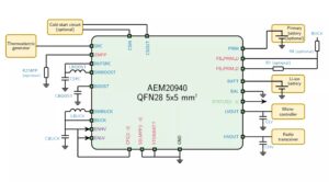
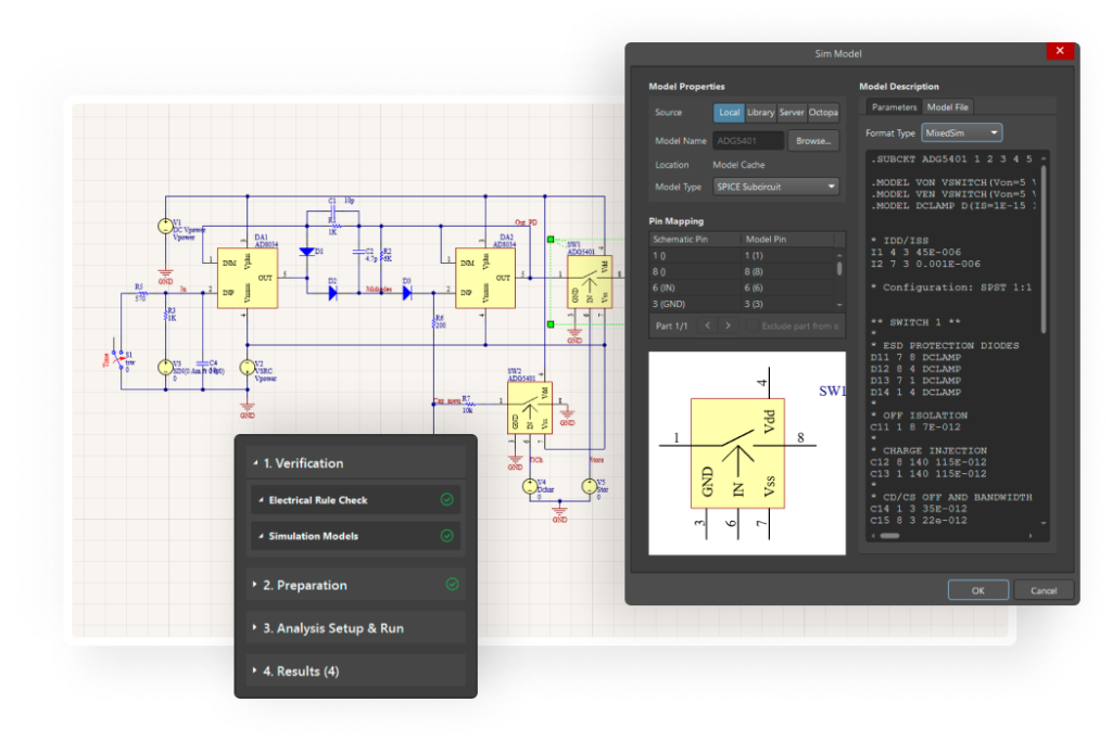
Simulation tools play a crucial role in ensuring a robust design. SPICE simulations can be used to validate the performance of power stages before physical implementation (Figure 3). Pre-compliance EMC testing should be conducted to identify potential issues early. Prototyping and testing thermal performance, voltage regulation, and noise levels are necessary steps to ensure the final product meets all requirements.
10 – Hints for improved performance
Several additional techniques can enhance the performance of power PCBs. Proper via design is essential for high-current paths, and multiple vias in parallel can help reduce resistance. Shielding techniques, such as copper pours or enclosures, can protect sensitive sections from noise. Using polygon pours for power nets improves current distribution, but adequate clearance should be maintained to prevent unintended coupling. The choice of PCB materials also matters; materials with a low dielectric constant and high thermal conductivity are preferable for power applications.
These considerations, when applied holistically, enable engineers to create efficient, reliable, and manufacturable PCB designs for power applications. Each step, from understanding requirements to final validation, contributes to a robust design that meets both performance and compliance standards.
Conclusion
In conclusion, designing PCBs for power applications is a multifaceted process that requires careful attention to electrical, thermal, and mechanical considerations. Starting with a clear understanding of the requirements ensures that all key parameters are addressed from the outset. Strategic component placement and routing are critical for minimizing noise, optimizing thermal performance, and ensuring power integrity.
Employing advanced simulation tools and adhering to industry standards for manufacturability and testing helps streamline the design process while ensuring compliance and reliability. Effective grounding, decoupling, and the use of dedicated planes contribute to reducing EMI and improving overall performance. Additionally, designing with future scalability and potential troubleshooting in mind, such as incorporating test points and clear labeling, can save time and resources during the validation phase. By integrating these principles and leveraging advanced materials and technologies, engineers can create PCBs that not only meet the functional requirements but also excel in efficiency and durability. Ultimately, the effort invested in meticulous planning and execution translates into robust, high-performance products that fulfill the demands of modern power electronics.

