Schottky Diode Drain Contact Interferences with Sub-Linearity
As the semiconductor industry improves, Schottky-Barrier MOSFETs with metallic source and drain connections are becoming more popular. Unlike ordinary impurity-doped silicon, the source and drain of Schottky-Barrier MOSFETs are constructed of silicide. When employing such devices in a logic circuit, the SB MOSFET has a unique behavior, such as an exponential current increase during Id -Vds triode operations, which happens when a moderate bias voltage is extremely unlikely [1]. The bandgap is the region of the semiconductor interface where Fermi-level pinning happens most frequently. As a result, the contact channel interfaces produce massive Schottky Barriers (SBs). This has a significant impact on the SB MOSFET’s electrical properties, resulting in poor ON-state performance and switching actions.
This page discusses the SB MOSFET’s qualities and characteristics, as well as why sub-linearity occurs on the source side rather than the drain side. Dual-gate silicon nanowire transistors with nickel silicide source and drain connections aided several tests and simulations.
This transistor can function in one of two ways. The first gate controls current flow initially, whereas the second applies a constant voltage larger than the maximum Vgs at gate 1. In the second operation, the program gate is at the source and the control gate is at the drain, where the fringing fields of both electrodes modulate the charge carrier concentration of the uncovered silicon channel (p-type, 10 15 cm 3) between the two gate electrodes, allowing the device to function properly.
SB MOSFET Simulation Parameters
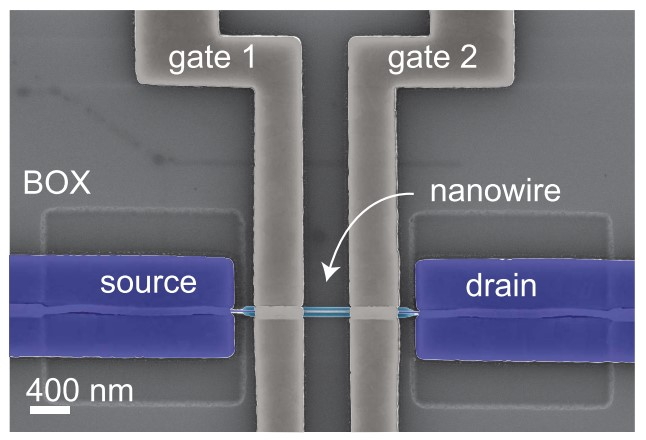
The non-equilibrium Green’s function formalism (NEGF) was used to study the sublinear Id -Vds behavior of SB-FETs using self-consistent Poisson-Schrödinger simulations. Figure 1 shows a nanowire field-effect transistor with metallic contacts and an SB Фs at the source and drain contacts.
The source and drain are assumed to be in touch with the nanowire, which not only depicts silicide connections but also contacts deposited on the nanowire and a strong metal nanowire coupling. A dnw nanowire was used for this experiment because it is thin enough to account for 1-D electronic transport and may be considered completely depleted over a wide range of channel doping doses. As a result, the inherent potential Фbi in channel doping changes. This device’s electrostatics can be altered using the Poisson equation.

The screening length scale for potential fluctuations is denoted by the above equation, where Фg + Ф bi are the gate and built-in potential energies, and Фf (x) is the potential energy at the channel dielectric interface. Furthermore, n(x) signifies the mobile charge density, and ε0 denotes the relative permittivity and vacuum of the nanowire.
SB MOSFET Simulation analysis
In the case of a single gate device, λ = ((εnw/εox)dnwdox)1/2 , where the same screening can be achieved with dnw = 1nm or dox = 4nm. Despite the fact that the charge density and potential are different in both circumstances, the screening length λ is the same. The sub-linearity feature can be minimized as dSB drops and the Schottky barrier at the drain end evaporates.
The quasi-Fermi level decreases on the source side, equivalent to the drain Fermi level. This behavior in the sub-linear surface is solely due to the source side of the Schottky Barrier. A large fraction of the applied bias drops across the drain Schottky Barrier. As a result, sublinear behavior occurs several times.
As dnw decreases dox increases, an increasing sublinear behavior develops. With a larger drain voltage, the charge-mediated impact of the potential distribution on the source side is greater. The carrier density falls and the oxide capacitance increases, resulting in a less substantial impact of the charge on the potential distribution.
Conclusion
The influence of charge in the channel on carrier injection through the source side of the SB MOSFET causes the sublinear increase in drain current as a function of Vds observed throughout the experiment. As VVds grows, the charge in the channel falls dynamically from the equilibrium value to a value equivalent to the transmission probability through the SB MOSFET’s source, according to the calculations. As the charge has a greater impact on the gain, the characteristic sublinear output behavior of SB MOSFETs was obvious. In the experiments, dual gate silicon nanowire SB MOSFET measurements were used.
References
[1] J. Knoch and B. Sun, “Sub-Linear Current-Voltage Characteristics of Schottky-Barrier Field- Effect Transistors,” in IEEE Transactions on Electron Devices, vol. 69, no. 5, pp. 2243-2247, May 2022, doi: 10.1109/TED.2022.3161245.
[2] B. Winstead and U. Ravaioli, “Simulation of Schottky barrier MOSFETs with a coupled quantum injection/Monte Carlo technique,” IEEE Trans. Electron Devices, vol. 47, no. 6, pp. 1241–1246, Jun. 2000, doi: 10.1109/16.842968.
[3] Z. Zhao, S. Rakheja, and W. Zhu, “Nonvolatile reconfigurable 2D Schottky barrier transistors,” Nano Lett., vol. 21, no. 21, pp. 9318–9324, Nov. 2021, doi: 10.1021/acs.nanolett.1c03557.
[4] ] E. J. Tan et al., “Demonstration of Schottky barrier NMOS transistors with erbium silicides source/drain and silicon nanowire channel,” IEEE Electron Device Lett., vol. 29, no. 10, pp. 1167–1170, Oct. 2008, doi: 10.1109/LED.2008.2004508.

