Short-circuit Failure Models for Silicon Carbide Devices

SiC power devices have emerged as a solution to the growing desire to reduce energy consumption at high switching frequencies. SiC devices can withstand high working temperatures, making it a good contender for the industrial setting. The availability of wide bandgap semiconductor devices has enabled engineers to construct power electronic systems to fulfil specific application needs [1]. Along with Silicon Carbide (SiC), Gallium Nitride (GaN) is a wide bandgap material. Cost, efficiency, power density, complexity, and dependability are all important considerations when constructing any power system [2].
Due to their quick switching rates and low on-state resistance, SiC MOSFETs are frequently damaged as a result of short-circuiting events [3]. A group of researchers from Anhui University of Technology’s School of Electrical and Information Engineering presented failure models of SiC devices in short-circuit cases on two commonly used power devices, SiC MOSFET (n-channel enhancement SiC MOSFET from Cree) and SiC JFET (normally-on SiC JFET from Infineon) [4].
Constructing SiC Transistor Failure Models
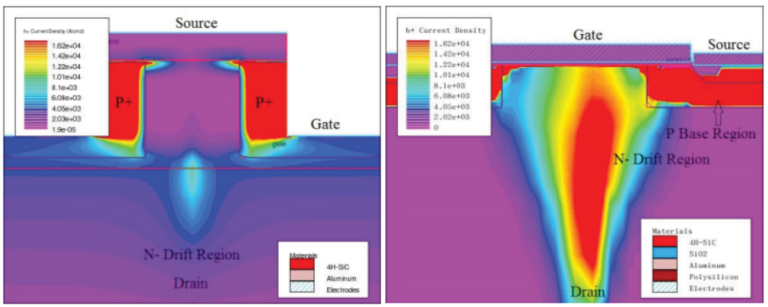
The investigation conducted by Z. Wang et al. demonstrates that under short-circuit conditions, the failure current is greater than the rated current of the power device [5]. The current component of SiC devices, particularly MOSFETs and JFETs represent the hole current density in both SiC transistors. We may deduce from the executed file that the high-density hole current passes through the PN junction between the transistors’ N – drift area and P base region.”TCAD simulation has also shown that, for SiC MOSFET, high-concentration carriers collect on the top of the JFET area, a percentage of which inject into the gate oxide and create the gate leakage current under the stress of high temperature and high electric-field strength,” the researchers say.
When developing the SiC JFET and SiC MOSFET failure models, the injection current leakage was an important parameter. The structure in the dotted boxes is typical of conventional circuit models, as is the supplementary current component,
I DS _LK was made in parallel connection with the channel current. I CH is the leakage current across the PN junction between the transistors’ N – drift region and P base region. According to the researchers, when there is no voltage bias on the gate to switch the device on.
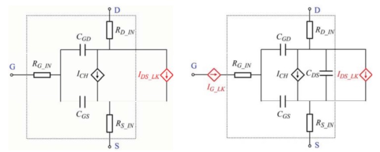
The thermal generation current Ith, avalanche current Iav, and diffusion current Idiff are the formulations for the leakage current via the PN junction. As a result, numerous strategies for reducing leakage current in the gate oxide have been proposed, including Fowler-Nordheim (FN) tunnelling and Poole-Frenkel (PF) emission. It is believed that the two currents, IPF and IFN, are a part of the SiC MOSFET gate oxide leakage current.
The Shichman-Hodges physical model was used to simulate SiC MOSFET circuits based on the SPICE level-1 model. While on the other hand, SiC JFET circuit modelling uses the Shockley physical model. Charge carriers in the channel can experience this impact as a result of higher current stress during short-circuit situations. This leads to a higher temperature than in the normal switching condition. In particular, SiC JFETs have a substantially longer failure time than a SiC MOSFETs. Leading to this, they also have a lower saturation current than a SiC MOSFET.
Validation of Failure Models of SiC Devices
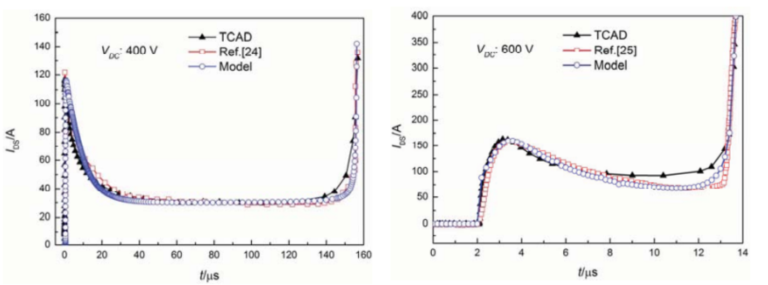
The created SiC JFET and SiC MOSFET failure models are validated under short-circuit fault conditions, with the figure illustrating a comparison of the failure currents produced from the models and the data provided in the study [6,7]. The results reveal that the short circuit failure time (tSC) for SiC JFET is 150s under 400V DC voltage and 13μs for SiC MOSFET under 600V DC voltage.
“The carrier mobility based on temperature and electric-field strength are required to appropriately create the SiC power device failure model,” the team writes. “Furthermore, by varying the combination mode of three current components of IDS _LK, a definite conclusion can be obtained that Ith affects whether or not the constructed model can mimic device failure.” As a result, the heat-generating current during short-circuit dominates the failure impact.
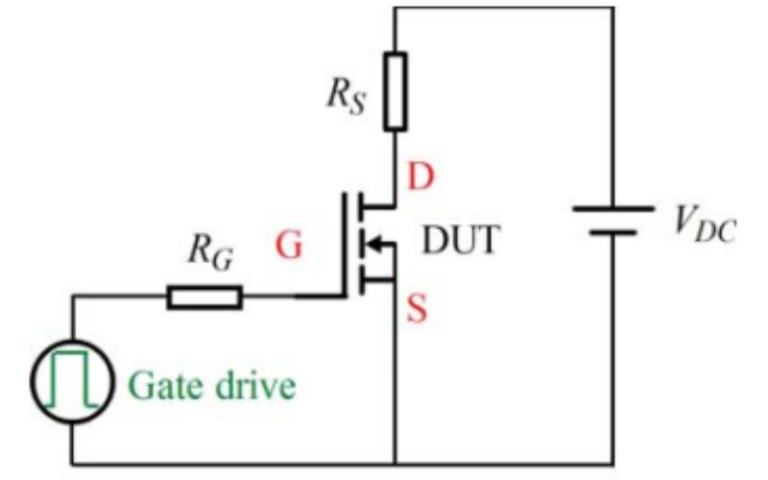
The schematic figure depicts the verification under short circuit fault conditions, with VDC representing the DC-link voltage, RS representing the stray resistance of the circuit loop, RG representing the gate resistance, and DUT representing the device (SiC JFET or SiC MOSFET). The image with red curves represents the first failure mode and blue curves represents the second failure mode. Two factors stand out: the lower saturation current of a SiC JFET than a SiC MOSFET and the much longer failure time of a SiC JFET than a SiC MOSFET. The temperature-dependent coefficient of carrier mobility is responsible for these variations.
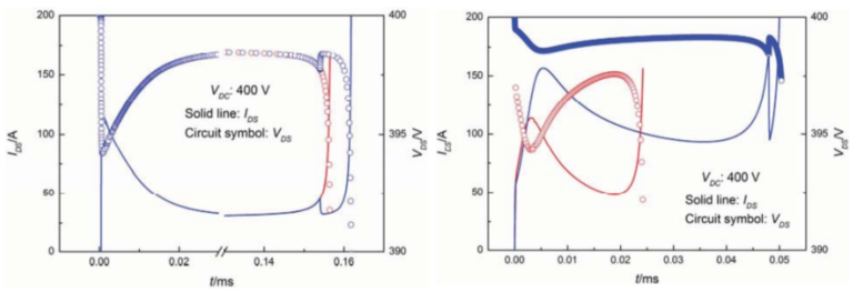
“SiC JFET has more short-circuit capacity than SiC MOSFET for instantaneous failure, but the failure duration and critical failure energy are both greater.” “The failure time of SiC JFET is much longer than that of SiC MOSFET for delayed failure at lower DC-link voltage, although the difference in failure time looks moderate at higher DC-link voltage,” the team discovers.
References
[1] A. K. Agarwal, “An overview of SiC power devices,” 2010 International Conference on Power, Control and Embedded Systems, 2010, pp. 1-4, doi: 10.1109/ICPCES.2010.5698670.
[2] H. Qin, B. Zhao, X. Nie, J. Wen and Y. Yan, “Overview of SiC power devices and its applications in power electronic converters,” 2013 IEEE 8th Conference on Industrial Electronics and Applications (ICIEA), 2013, pp. 466-471, doi: 10.1109/ICIEA.2013.6566414.
[3] B. J. Nel and S. Perinpanayagam, “A Brief Overview of SiC MOSFET Failure Modes and
Design Reliability,” Procedia CIRP, vol. 59, pp. 280–285, 2017, doi:
[4] Y. Zhou, T. Yang, H. Liu and B. Wang, “Failure Models and Comparison on Short-circuit Performances for SiC JFET and SiC MOSFET,” 2018 1st Workshop on Wide Bandgap Power Devices and Applications in Asia (WiPDA Asia), 2018, pp. 123-129, doi:10.1109/WiPDAAsia.2018.8734661.
[5] Z. Wang et al., “Temperature-Dependent Short-Circuit Capability of Silicon Carbide Power MOSFETs,” in IEEE Transactions on Power Electronics, vol. 31, no. 2, pp. 1555-1566, Feb.2016, doi: 10.1109/TPEL.2015.2416358.


