Five-level single-phase SiC converter reduces switch voltage stress
With the advancement of new technologies, there is a greater demand for devices with high performance and efficiency. Despite traditional Multilevel converters (MLC) meeting these requirements, they fall short in other areas, such as requiring a large number of power electronics switches, supporting circuits, and the complexity of their system. All of these issues contribute to the issue of higher costs and cumbersome systems. This article discusses an effective MLC modification that uses advanced technologies to improve a classic SiC converter.
A multilevel SiC converter (MLC) is a technology for producing high-voltage waveforms from low-voltage components. It employs gadgets that require a moderate quantity of power and provides applications in fields that require a high level of power. MLCs provide several advantages, including improved output waveforms, reduced harmonics, and decreased switching losses. They are the ideal solution when a large amount of power with a low/medium voltage range is required. MLC SiC converters can be used in industrial AC-AC applications to supply sine-wave input currents with unity power factor in regulators and protect sensitive appliances such as computers, medical instruments, and communication settings from low-quality supplies. In the gas, oil, mining, and marine industries, DC-AC MLCs are employed. These MLCs are great efficiency solutions in renewable energy low-power applications.
MLC topologies are classified into three types: flying capacitor (FC), neutral-point-clamped (NPC), and cascaded H-bridge. The NPC type topology can be redesigned to create the T-type topology. Although this topology minimizes conduction losses (a disadvantage of NPC), it still has substantial switching losses. Following that, researchers provided a five-level system with switch voltage stress minimization simply by altering the three-level T-type. It has all of the advantages of T-type with the addition of waveform improvisation and harmonic reduction. After further modification, a system focusing on high switching losses was presented: a T-type extremely efficient converter with SiC MOSFETs replacing the outer switches.
Formation of T-type Topology
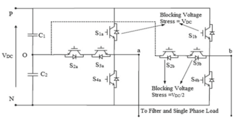
The diagram above depicts a common single-phase inverter made up of three-level T-type legs. It has eight power devices, namely S 1a – S 4a and S 1b – S 4b, as well as anti-parallel diodes. This circuit can be configured with either common emitter (CE) or common collector (CC) three-level legs (CC). Employing this, two unique legs can be introduced, as shown below, using two SiC MOSFET switches in the outer and two Si MOSFETs of lesser rating as bidirectional switches.
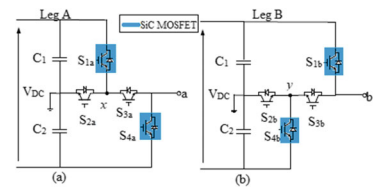
In figure (a), one modified leg (leg A) is produced by connecting the terminals of S1a, S 2a collector terminal, and S3a collector terminal at point “x.” This is a bidirectional switch’s common collector (CC) configuration. Similarly, the other modified leg (leg B) is produced at point “y” using S4a, the emitter terminal of switch S2a, and the emitter terminal of S3a, and this configuration is a common emitter (CE) arrangement of bi-directional switches, as shown in figure (b).
Five-level Single-Phase T-Type Inverter Operating Parameters
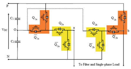
A five-level single-phase T-type inverter circuit is depicted in the above diagram. Two sophisticated modified three-level T-type legs make up each leg. Since there is no clamping diode, the circuit is simpler. Three voltage levels can be found in the voltage level acquired at Va0 and Vb0, and five voltage levels can be found in the voltage level obtained as an output, as determined by the formula,
V_ab = V_a0 − V_b0
Symmetry is obtained for simple control, necessitating complementary logic, which is accomplished by selecting an appropriate switch numbering. Switching limits are established to simultaneously stop conduction. As a result, + = 1 with x = 1, 2 and y = a, b.
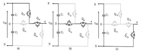
The switching state circuit of the novel inverter leg A is depicted in the figure above. If the respective switch is closed, Qx y is 1, otherwise, it is 0. The phase current flows from one of the DC-node link’s points. The respective capacitor voltage will be output on the AC side depending on the switching state. Further investigation reveals that a novel T-type inverter facilitates suppression of total voltage stress on the switch of inverter legs A and B. Another advantage is that legs A and B are independent of one another and can be used to form a poly-phase converter.
Five-level single-phase T-type SiC converter simulation results
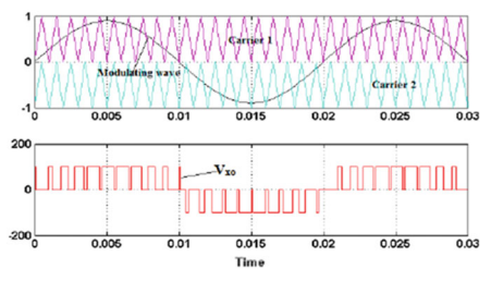
Various modulation techniques, including pulse width modulation (PWM) schemes used in other topologies, can be used. However, in this article, we will concentrate on phase disposition (PD) modulation, as illustrated in the figure above. Switching signals for, and are generated by using wave 1 and wave 2 as carrier waves, respectively. The sinusoidal modulation wave is 180° out of phase.
The phase disposition modulation technique was used to simulate a T-type five-level single-phase converter. On the output side, a load of 125 V, 1 kVA, 0.8 lag pf, 50 Hz was connected, and a DC-link voltage of 200 V was used. According to the results, during the positive voltage from leg A, full DC-link voltage stress appeared only across (Q2a), and during the negative voltage from leg B, full DC-link voltage stress appeared only across (Q1b). The figure below depicts the novel converter’s outputs from one leg and voltage output.
Si vs SiC Converter – Five-Level Topology Comparison
When comparing the novel T-type topology to conventional T-type, NPC, FC, and CHB topologies, various factors such as component requirements, isolated supplies, clamping diode requirements, and so on are taken into account. The number of main switches is nearly equal, but in a few topologies, clamping diodes and capacitors are eliminated. This novel T-type topology also focuses on voltage stress reduction and replaces the conventional Si switch with a more advantageous SiC switch. So, in addition to reducing stress and minimizing switch count, switching frequency for the same losses can be increased, improving the converter’s efficiency and reliability.

Conclusion
The simulation results demonstrate that this T-type topology is applicable within the desired permissible limits. It offers advantages such as fewer clamping switches and a reduction in bidirectional switches. The switching voltage stress in this novel T-type legs topology is lower than in conventional T-type. These independent legs can be used to create a poly-phase system, and H-bridge cells can be used to achieve a higher voltage level. Additionally, losses can be calculated and compared to conventional topologies, and a highly efficient inverter and AC-DC-AC converter can be implemented. As a result, these studies could be conducted to reduce the voltage impact on the switch, which is still subjected to full voltage stress.

