GaN on Si power technology: its scope and potential
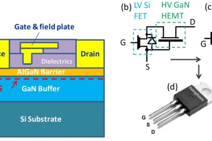
Gallium Nitride (GaN) has demonstrated tremendous potential over silicon(si) in the field of semiconductor technology for a wide range of high-power applications in recent years. When compared to silicon-based semiconductor devices, Gallium Nitride has a higher breakdown strength and thermal conductivity. Moreover, it is a physically hard and stable Wide Bandgap (WBG) semiconductor with fast switching speeds and higher electrical conductivity.
Gallium Nitride crystals can be grown on a variety of substrates, including sapphire, silicon carbide (SiC), silicon (Si), and others. By doing so on Silicon, the existing fabrication infrastructure can be used, eliminating the need for expensive production sites and taking advantage of cheap large-diameter Silicon wafers.
As a result, GaN on silicon has a wide range of future applications, extending current HEMT capabilities with improved power levels above 1kW. This technology enables designers to increase operating voltages and extend frequency response beyond the Ka-band into the E-band, W-band, and terahertz space. This theory was presented by a team of researchers from the department of electronics and computer technology at the Hong Kong University of Science and Technology.
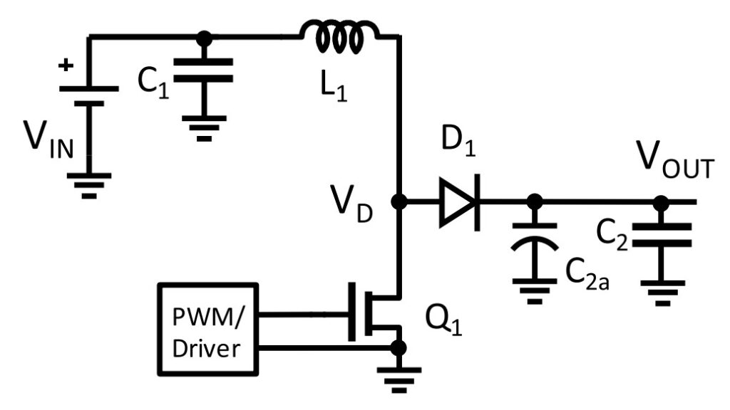
The illustration above depicts a 600V class GaN on a Si device with a boost converter and a fast diode. In the circuit, the switching device Q1 and the boost diode D1 are shown, along with input and output capacitors C1 and C2 for improved voltage stabilization. When Q1 is turned on, the input voltage is applied to L1 whereas when Q1 is turned off, diode D1 releases the stored energy to the output. Moving on, Continuous conduction and discontinuous conduction are the two modes of operation. In the continuous conduction mode, the inductor current remains above zero, whereas in the discontinuous conduction mode, the inductor completely releases its stored energy.
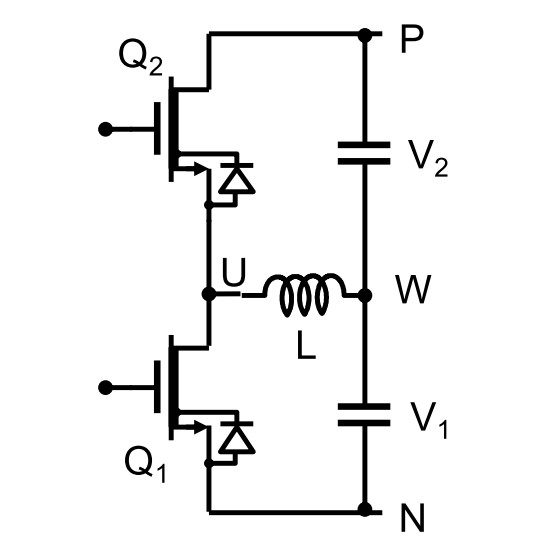
Both Q1 and Q2 in the above figure are GaN Cascode devices that are capable of blocking reverse conductivity voltage when the gate is turned off. When the gate is in ON conduction, the corresponding device provides the best forward and reverse conductivity with the least voltage drop. With the addition of an inductor L between a switching node U and a DC or low-frequency middle potential W, the half-bridge can be configured as a boost converter, buck converter, or dc-ac inverter.
To improve performance, a boost converter with 600 V/52 m GaN cascade switches and 650 V/43 m state-of-the-art Si SJ MOSFETs optimized for low Q was tested. However, during the experiment, it was discovered that all circuit components, with the exception of switching devices, were the same.
Scope of GaN-on-Si in the field of power electronics
In simple space hard-witched mode, GaN on Si can operate at high frequencies as well as high power levels. This provides low loss during operation, which will be important in the coming years for power conversions and will have an impact on applications such as servo motor drives, compact EV chargers, and so on. GaN-on-Si is currently used in satellites, LIDAR for autonomous vehicles, augmented reality systems, robotics, and other applications. GaN transistors and integrated circuits (ICs) are already commercially available and are 5 to 50 times faster than analogous silicon state-of-the-art devices.
Except for efficiency and performance, GaN transistors are very similar to other conventional power MOSFETS on the market today. This allows power system engineers and other technicians to design circuits with little additional training. However, any parasitic inductions in the circuit must be given special consideration and should be treated carefully.
Due to the fact that GaN devices are smaller in size, tighter assembly tolerances are required, similar to those used in computer and telecom devices. Once designed and manufacturing professionals become more familiar with the smaller and more efficient GaN devices, the technology has proven to integrate smoothly into the infrastructure designed for silicon MOSFETs.
As GaN devices are significantly smaller than their silicon counterparts, more devices can be manufactured at the same time. Furthermore, because GaN transistors are low-voltage transistors (500V), they do not require the same expensive packaging as silicon MOSFETs. Additionally, design engineers can expect further price reductions as GaN technology research is completed in the coming years, giving these systems a growing market advantage over traditional silicon-based devices.
Growth of GaN transistors in the industry
Several GaN transistor manufacturers have reported exceptional results during in-house stress testing and performance experience as of today. Aside from that, a large number of GaN transistors have gone through billions of accumulated hours in actual on-ground applications, demonstrating higher field reliability when compared to silicon MOSFETs.
Therefore, it is safe to say that GaN-on-Si device technology has demonstrated impressive performance in ON-resistance, switching speed, thermal performance, chip size, and cost. The rapid advancement of GaN power semiconductors will result in even more miniaturization of power electronic subsystems and an increase in efficiency.
References
[1] K. J. Chen et al., “GaN-on-Si Power Technology: Devices and Applications,” in IEEE Transactions on Electron Devices, vol. 64, no. 3, pp. 779-795, March 2017, DOI: 10.1109/TED.2017.2657579.
[2] M. Ishida, T. Ueda, T. Tanaka, and D. Ueda, “GaN on Si technologies for power switching devices,” IEEE Trans. Electron Devices, vol. 60, no. 10, pp. 3053–3059, Oct. 2013.
[3] K. Y. Wong, W. Chen, and K. J. Chen, “Integrated voltage reference and comparator circuits for GaN smart power chip technology,” in Proc. 21st Int. Symp. Power Semiconductor Devices IC’s, Oct. 2009, pp. 57–60.
[4] K. V. Smith, J. Haller, J. Guerrero, R. P. Smith, R. Lal, and Y.-F. Wu, “Lifetime tests of 600-V GaN-on-Si power switches and HEMTs,” Microelectron. Reliab., vol. 58, pp. 197–203, Mar. 2016.

